
AES Hardware Accelerator
Introduction
For this lab, we implemented an AES hardware accelerator, using an FPGA to accelerate and controlling it with an MCU controller.
Design and Testing Methodology
To test this lab, there were built in testbenches that I used, including an testbench_aes_core.sv, an testbench_aes_spi.sv, and also an testbench_aes_spi.sv file.
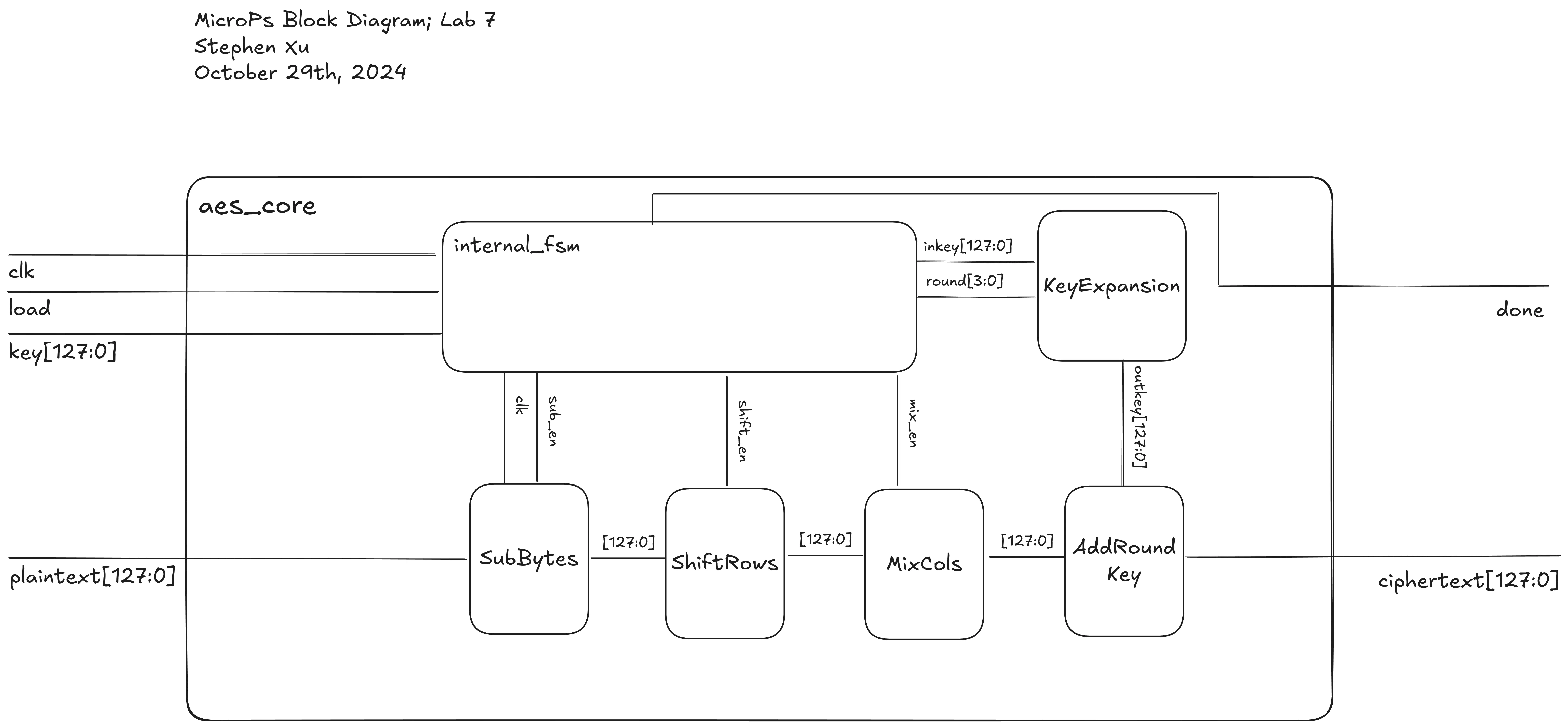
To design the hardware accelerator part of the FPGA, I chose to take a cue for the datapath design in E85, treating the AES encryption cycle as a multicycle processor, and substituting the AES encryption steps as basically a more complicated ALU.
We could not use combinational logic for this (or at least not easily), as the SBOX would be too big to fit fully combinationally, and would instead operate much better.
I could pretty much tell that the code was working, when I sent over the data via the MCU, and received data from the FPGA, but the testbenches were very helpful in telling if the intermediate encryptions were correct. The test cases I used were from the NIST manual, and showed step by step what the intermediate values were as it went through different rounds of AES.
Testbenches
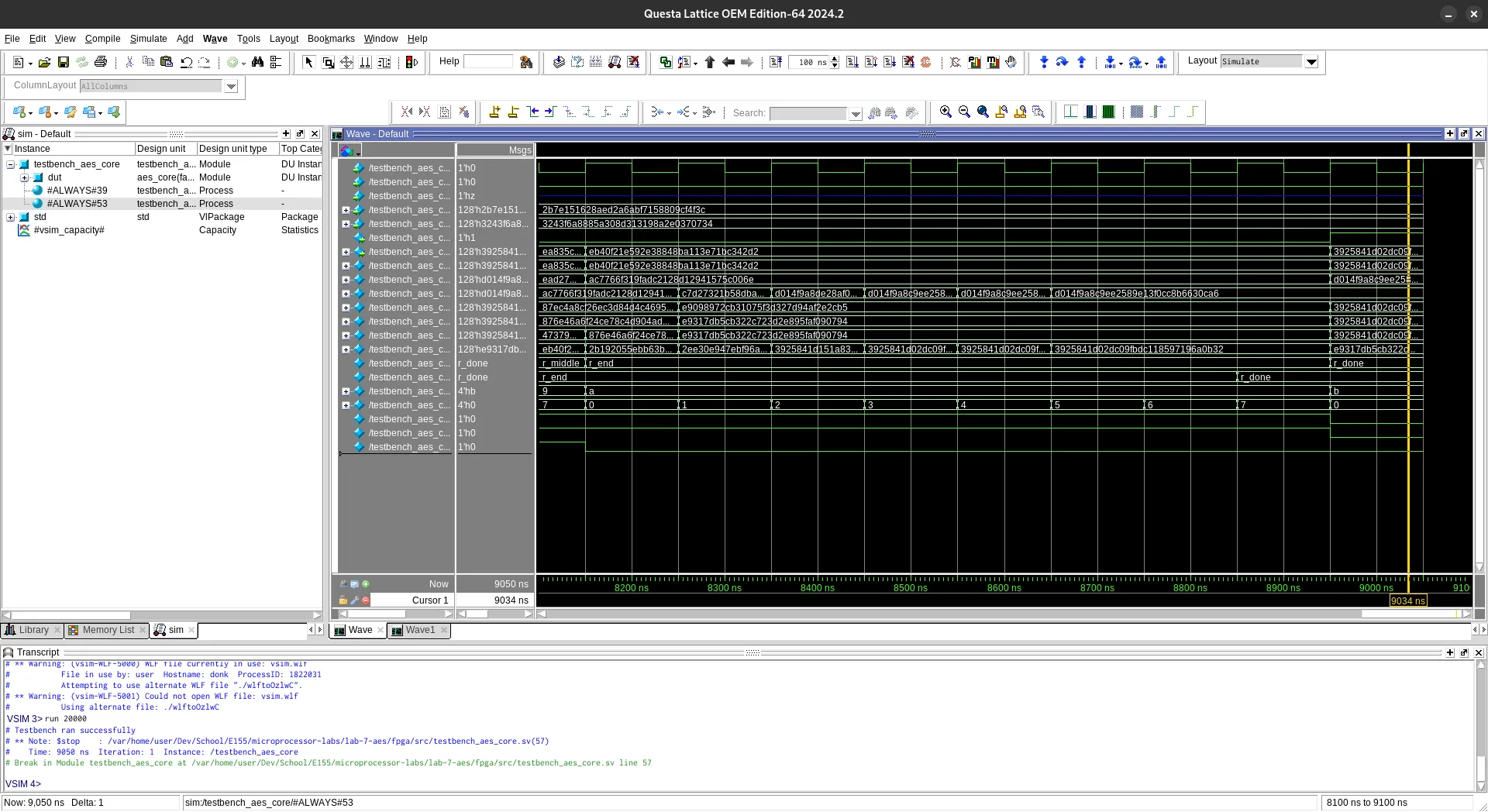
Testbench testing the core AES logic:
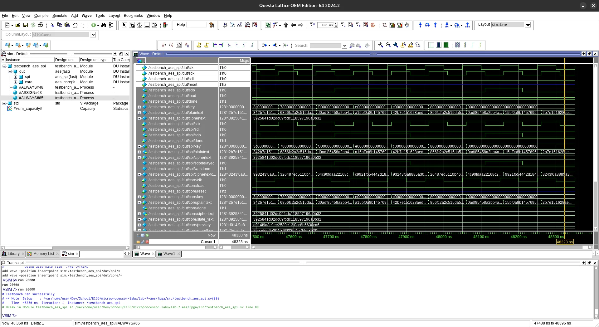
And another testbench testing the AES logic with SPI:
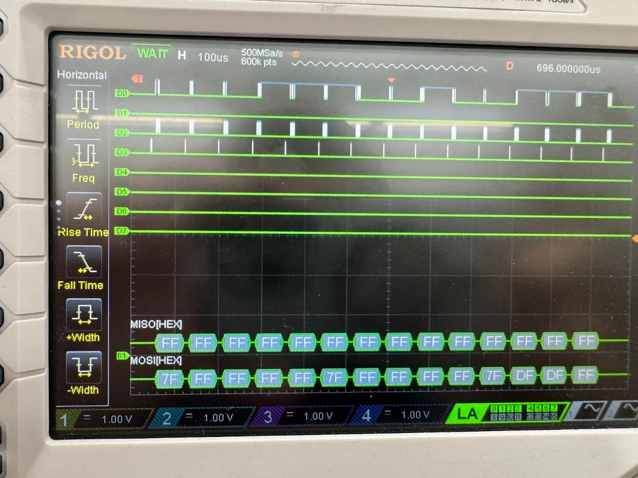
Logic Analyzer
And here is a picture of the Logic Analyzer output attached to the SPI pins.
Technical Documentation:
The source code for this project can be found in my Github Repository.
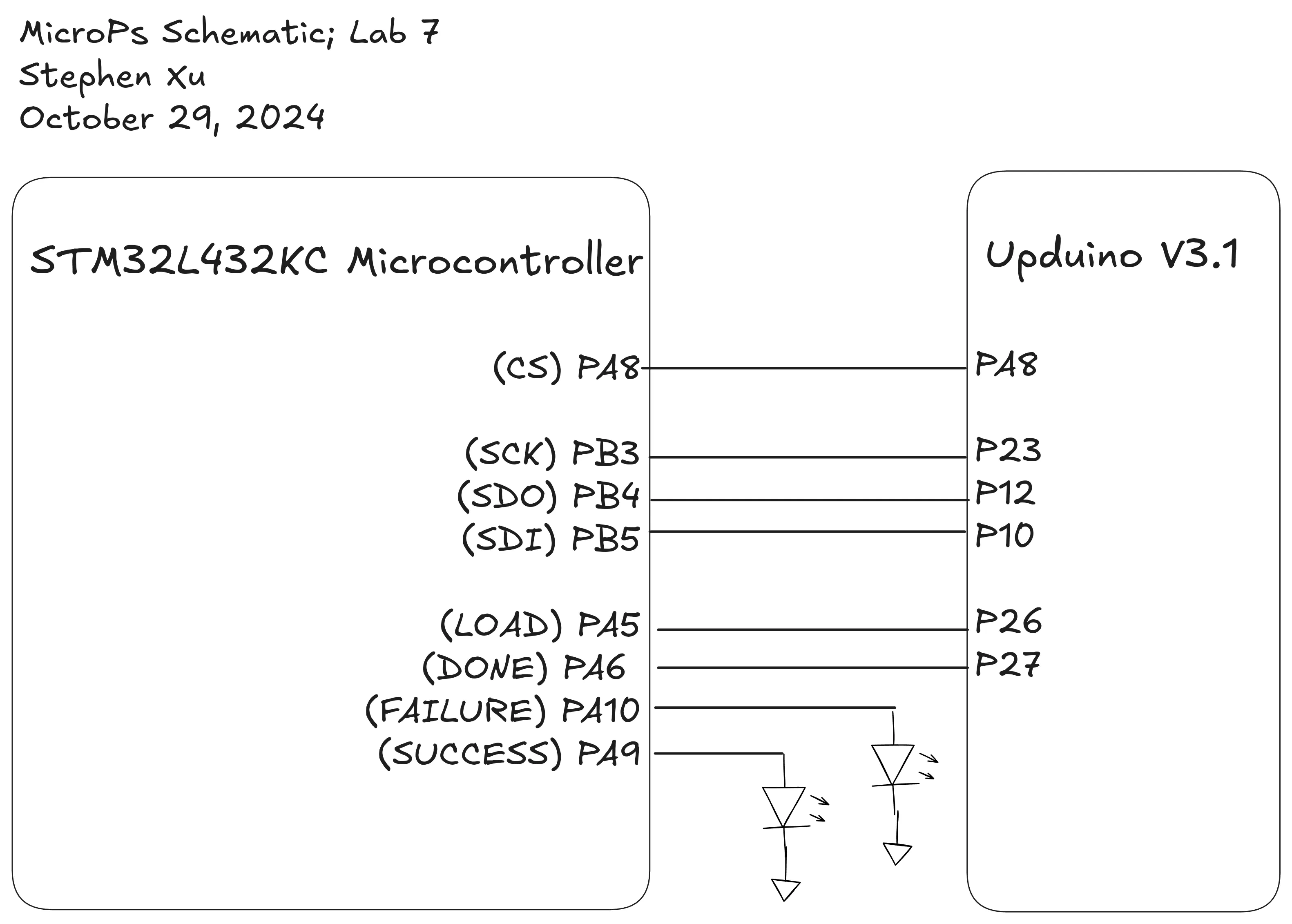
Schematic
Below is a schematic demonstrating the connection between the microprocessor and the FPGA, as well as debug LEDs.
Block Diagram
Here is the block diagram of AES encryption on the FPGA.
Feedback
The starter code my class had was very messy, which was definitely not great. There were misspellings such as cyphertext instead of ciphertext, and putting all the SystemVerilog modules in one file, which I found to be really annoying and had to spend some time going through and modifying.
Conclusion
I was expecting this lab to not take me very long, as I already knew a lot about AES beforehand. However, it still took me around 20 hours, although I was able to get it working in simulation quite quickly this time. I ended up staying up until 5:30 am the night before this lab was due, getting it to work. This lab did go a lot smoother than the last FPGA lab I did, and I was able to diagnose the hardware issues much faster, which is a good sign.